olo_base_fifo_async
Status Information
VHDL Source: olo_base_fifo_async
Description
This component implements an asynchronous FIFO (different clocks for write and read port).
The memory is described in a way that it utilizes RAM resources (Block-RAM or distributed RAM) available in FPGAs with commonly used tools. For this purpose olo_base_ram_sdp is used.
The FIFO is a fall-through FIFO and has AXI-S interfaces on read and write side.
The RAM behavior (read-before-write or write-before-read) can be selected. This allows efficiently implementing FIFOs for different technologies (some technologies implement one, some the other behavior).
An asynchronous FIFO is a clock-crossing and hence this block follows the general clock-crossing principles. Read through them for more information.
Note: This is a symmetric FIFO. To build an asymmetric n:xn FIFO (N-bits to a multiple of N-bits), the olo_base_wconv_n2xn can be added on the write side of the FIFO. To create an xn:n FIFO (a multiple of N-bits to N-bits), the olo_base_wconv_xn2n can be added on the read side of the FIFO.
Generics
| Name | Type | Default | Description |
|---|---|---|---|
| Width_g | positive | - | Number of bits per FIFO entry (word-width) |
| Depth_g | positive | - | Number of FIFO entries. This must be a power of two. See Architecture for more details. |
| AlmFullOn_g | boolean | false | If set to true, the AlmFull (almost full) status flag is generated (otherwise it is omitted) |
| AlmFullLevel_g | natural | 0 | Level to generate AlmFull flag at. Has no effect if AlmFullOn_g = false |
| AlmEmptyOn_g | boolean | false | If set to true, the AlmEmpty (almost empty) status flag is generated (otherwise it is omitted) |
| AlmEmptyLevel_g | natural | 0 | Level to generate AlmEmpty flag at. Has no effect if AlmEmptyOn_g = false |
| RamStyle_g | string | "auto" | Through this generic, the exact resource to use for implementation can be controlled. This generic is applied to the attributes ram_style and ramstyle which vendors offer to control RAM implementation. For details refer to the description in olo_base_ram_sdp. |
| RamBehavior_g | string | "RBW" | "RBW" = read-before-write, "WBR" = write-before-read For details refer to the description in olo_base_ram_sdp. |
| ReadyRstState_g | std_logic | '1' | Controls the status of the In_Ready signal in during reset. Choose '1' for minimal logic on the (often timing-critical) In_Ready path. |
| Optimization_g | string | "SPEED" | "LATENCY" - optimize for minimum time until a word written is showing up at the output "SPEED" - optimize for highest possible clock speed (at the cost of more latency) |
| SyncStages_g | positive | 2 | Number of synchronization stages. Note that more synchronization stages also mean a higher latency until written data is visible on the read side. Range: 2 ... 4 |
Interfaces
Input Data
| Name | In/Out | Length | Default | Description |
|---|---|---|---|---|
| In_Clk | in | 1 | - | Input clock |
| In_Rst | in | 1 | - | Reset input (high-active, synchronous to In_Clk) |
| In_RstOut | out | 1 | N/A | Reset output (see clock-crossing principles, synchronous to In_Clk)) |
| In_Data | in | Width_g | - | Input data (synchronous to In_Clk) |
| In_Valid | in | 1 | '1' | AXI4-Stream handshaking signal for In_Data (synchronous to In_Clk) |
| In_Ready | out | 1 | N/A | AXI4-Stream handshaking signal for In_Data (synchronous to In_Clk) |
Output Data
| Name | In/Out | Length | Default | Description |
|---|---|---|---|---|
| Out_Clk | in | 1 | - | Output clock |
| Out_Rst | in | 1 | - | Reset input (high-active, synchronous to Out_Clk) |
| Out_RstOut | out | 1 | N/A | Reset output (see clock-crossing principles, synchronous to Out_Clk)) |
| Out_Data | out | Width_g | N/A | Output data (synchronous to Out_Clk) |
| Out_Valid | out | 1 | N/A | AXI4-Stream handshaking signal for Out_Data (synchronous to Out_Clk) |
| Out_Ready | in | 1 | '1' | AXI4-Stream handshaking signal for Out_Data (synchronous to Out_Clk) |
Input Status
| Name | In/Out | Length | Default | Description |
|---|---|---|---|---|
| In_Full | out | 1 | N/A | Status flag. Asserted if the FIFO is full (synchronous to In_Clk) |
| In_Empty | out | 1 | N/A | Status flag. Asserted if the FIFO is empty (synchronous to In_Clk) |
| In_AlmFull | out | 1 | N/A | Status flag. Asserted if the FIFO fill level is >= AlmFullLevel_g (synchronous to In_Clk) Output is undefined if AlmFullOn_g=false. |
| In_AlmEmpty | out | 1 | N/A | Status flag. Asserted if the FIFO fill level is <= AlmEmptyevel_g (synchronous to In_Clk) Output is undefined if AlmEmptyOn_g=false. |
| In_Level | out | ceil(log2(Depth_g+1)) | N/A | FIFO fill level calculated on the write side (synchronous to In_Clk) |
Output Status
| Name | In/Out | Length | Default | Description |
|---|---|---|---|---|
| Out_Full | out | 1 | N/A | Status flag. Asserted if the FIFO is full (synchronous to Out_Clk) |
| Out_Empty | out | 1 | N/A | Status flag. Asserted if the FIFO is empty (synchronous to Out_Clk) |
| Out_AlmFull | out | 1 | N/A | Status flag. Asserted if the FIFO fill level is >= AlmFullLevel_g (synchronous to Out_Clk) Output is undefined if AlmFullOn_g=false. |
| Out_AlmEmpty | out | 1 | N/A | Status flag. Asserted if the FIFO fill level is <= AlmEmptyevel_g (synchronous to Out_Clk) Output is undefined if AlmEmptyOn_g=false. |
| Out_Level | out | ceil(log2(Depth_g+1)) | N/A | FIFO fill level calculated on the write side (synchronous to Out_Clk) |
Architecture
The rough architecture of the FIFO is shown in the figure below. Note that the figure does only depict the general architecture and not each and every detail.
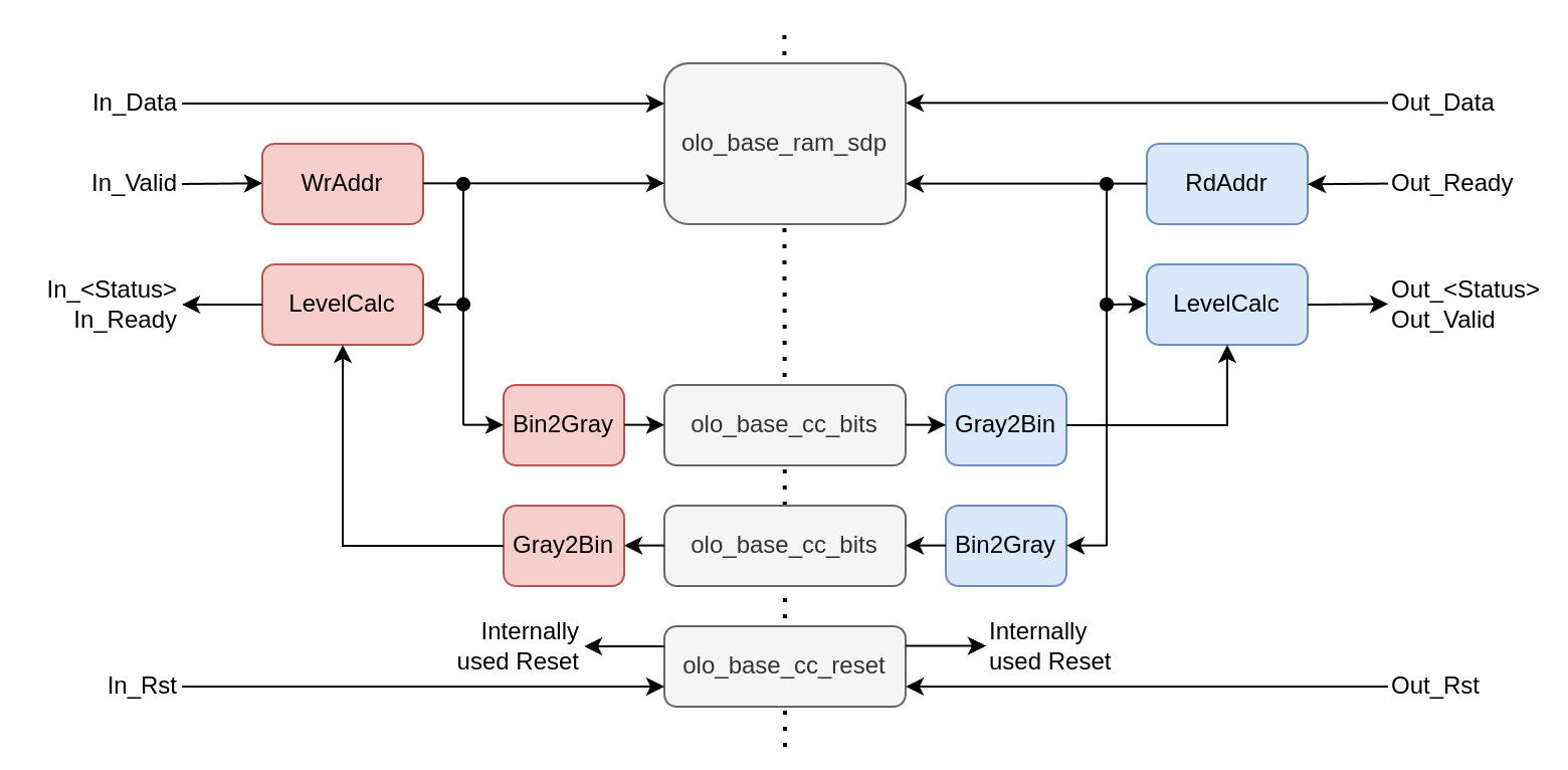
Read and write address counters are handled in their corresponding clock domain. The current address counter value is then transferred to the other clock-domain by converting it to gray code, synchronizing it using aa synchronizer (using olo_base_cc_bits) and convert it back to a two's complement number. Because the data is transferred in gray code, in this case either the correct value before an increment of the counter or the correct value after the increment is received, so the result is always correct.
The gray-encoding approach only works for power of two FIFO depths. For any other FIFO depths, the gray encoded counter value would toggle more than one bit during the overflow and hence the clock domain crossing would not work safely.
All status information is calculated separately in both clock domains to make it available synchronously to both clocks.
This architecture is independent of the FPGA technology used and can also be used to combine more than just one Block-RAM into one big FIFO.
Regarding constraints, refer to clock-crossing principles. The FIFO is also auto-constraints capable.
Architecture
The control logic (pointers, level/flag detection, optimization pipeline) lives in a private entity
olo_private_fifo_async_core, which exposes the storage RAM and the Gray-pointer/reset clock-crossings as ports. This
entity supplies the standard olo_base_cc_bits / olo_base_cc_reset
crossings and an olo_base_ram_sdp. The fault-tolerant variant
olo_ft_fifo_async reuses the same core but supplies TMR-hardened CDC primitives and adds
ECC for data-path protection, so this base entity carries no fault-tolerance dependency.