olo_ft_ram_sdp
Status Information
VHDL Source: olo_ft_ram_sdp
Description
This component implements an ECC-protected simple dual-port RAM using SECDED (Single Error Correction, Double Error Detection) Hamming code. It wraps olo_base_ram_sdp internally with a wider word to store parity bits alongside data.
The ECC is transparent to the user: data is automatically encoded on write and decoded/corrected on read. Error status flags indicate whether a single-bit error was corrected or a double-bit error was detected.
The simple dual-port topology has one dedicated write port and one dedicated read port. The two ports may share a clock or run on independent clocks (set IsAsync_g = true to give the read port its own Rd_Clk).
For an opportunistic background memory scrubber, use olo_ft_ram_sdp_scrub, a separate entity that wraps this one plus the scrubber FSM. The scrub variant is sync-only (no IsAsync_g).
For background on the SECDED scheme, the codeword layout, error injection semantics and the constraints that apply across the ft area, see Open Logic Fault-Tolerance Principles.
Generics
| Name | Type | Default | Description |
|---|---|---|---|
| Depth_g | positive | - | Number of addresses the RAM has |
| Width_g | positive | - | Number of data bits stored per address (word-width). The internal RAM is wider to accommodate ECC parity bits. |
| IsAsync_g | boolean | false | When true, the read port runs on a separate clock (Rd_Clk / Rd_Rst). When false, the read port shares Clk / Rst with the write port. |
| RamRdLatency_g | positive | 1 | Read latency of the wrapped RAM, excluding ECC pipeline stages. Higher values can help close timing on the RAM read path. |
| RamStyle_g | string | "auto" | Controls the RAM implementation resource. Passed through to olo_base_ram_sdp. |
| RamBehavior_g | string | "RBW" | Controls the RAM behavior. "RBW": Read-before-write "WBR": Write-before-read |
| EccPipeline_g | natural | 0 | Number of pipeline register stages within the ECC decoder (range 0..2). 0 = combinational decode (default). 1 = single register at the decoder output - breaks the path from the RAM read port to the user's logic. 2 = distributed pipeline: register between syndrome compute and correction, plus a register at the output - use this when both halves of the SECDED logic need their own clock cycle to close timing. See ECC Pipeline for details. Total read latency is RamRdLatency_g + EccPipeline_g cycles. |
Interfaces
Clock and Reset
| Name | In/Out | Length | Default | Description |
|---|---|---|---|---|
| Clk | in | 1 | - | Write-side clock (also the read clock when IsAsync_g = false). |
| Rst | in | 1 | '0' | Reset (high-active, synchronous to Clk). Clears the internal error-injection latch and the read-valid pipeline. The stored RAM contents are unaffected (block RAMs cannot be reset). |
| Rd_Clk | in | 1 | '0' | Read-side clock. Only used when IsAsync_g = true, otherwise Clk is used for the read port. |
| Rd_Rst | in | 1 | '0' | Read-side reset (high-active, synchronous to Rd_Clk). Only used when IsAsync_g = true. Clears the read-valid pipeline on the read side; RAM contents are unaffected. |
Write Port
| Name | In/Out | Length | Default | Description |
|---|---|---|---|---|
| Wr_Addr | in | ceil(log2(Depth_g)) | - | Write address |
| Wr_Ena | in | 1 | '1' | Write enable |
| Wr_Data | in | Width_g | - | Write data |
Read Port
| Name | In/Out | Length | Default | Description |
|---|---|---|---|---|
| Rd_Addr | in | ceil(log2(Depth_g)) | - | Read address |
| Rd_Ena | in | 1 | '1' | Read enable. Rd_Valid pulses '1' exactly RamRdLatency_g+EccPipeline_g cycles after each Rd_Ena = '1' cycle. Leave at the default '1' for continuous reads. |
| Rd_Data | out | Width_g | N/A | Read data (corrected if a single-bit error was detected) |
| Rd_Valid | out | 1 | N/A | Read-data valid. Pulses '1' when Rd_Data / Rd_EccSec / Rd_EccDed correspond to a read (= Rd_Ena delayed by RamRdLatency_g+EccPipeline_g cycles). |
| Rd_EccSec | out | 1 | N/A | Single error corrected flag. '1' when a single-bit error was detected and corrected. |
| Rd_EccDed | out | 1 | N/A | Double error detected flag. '1' when an uncorrectable double-bit error was detected. Read data is unreliable in this case. |
Error Injection (optional)
These ports drive the internal olo_ft_ecc_encode instance. Leave them unconnected for normal operation; see Open Logic Fault-Tolerance Principles - Error Injection for the latched-strobe semantics shared across the ft area.
| Name | In/Out | Length | Default | Description |
|---|---|---|---|---|
| ErrInj_BitFlip | in | eccCodewordWidth(Width_g) | all 0 | Codeword-wide flip pattern. Each '1' bit XORs (flips) the corresponding bit of the stored codeword. Popcount 1 = SEC-correctable, popcount 2 = DED-detectable. |
| ErrInj_Valid | in | 1 | '0' | Strobe that latches ErrInj_BitFlip into the encoder's pending-injection register. The latched pattern is applied to the next write. If ErrInj_Valid = '1' and Wr_Ena = '1' in the same cycle the pattern is applied directly without going through the latch. |
Detailed Description
Architecture
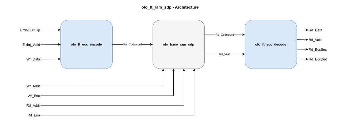
The ECC encoding is combinational on the write path. The internal RAM (an instance of olo_base_ram_sdp with a
codeword-wide word) provides the configurable read pipeline (RamRdLatency_g) and forwards its Rd_Valid to the
decoder. The ECC decoding happens in the internal olo_ft_ecc_decode instance and the error
flags are time-aligned with the read data regardless of EccPipeline_g.
When IsAsync_g = true the read port (RAM read side and the decoder) runs on Rd_Clk / Rd_Rst; the write path (the encoder and the RAM write side) always runs on Clk / Rst.
ECC Pipeline
EccPipeline_g is forwarded one-to-one to the internal olo_ft_ecc_decode instance and
inserts register stages on the decode datapath. The range is 0..2:
EccPipeline_g |
Structure |
|---|---|
| 0 | Combinational decode after the RAM read port. Rd_Data / Rd_EccSec / Rd_EccDed appear RamRdLatency_g cycles after Rd_Addr. |
| 1 | Combinational syndrome + correction + SEC/DED → register near the output. Breaks the path from the RAM read port to the user's logic. |
| 2 | Combinational syndrome → register → combinational correction + SEC/DED → register. Breaks both the syndrome path and the correction path - use this when both halves of the SECDED logic need their own clock cycle to close timing at high clock frequencies. |
Total read latency from address-presented to data-valid is RamRdLatency_g + EccPipeline_g clock cycles.
ECC Overhead, Error Injection and Status Flags
See the corresponding sections in Open Logic Fault-Tolerance Principles:
- ECC Overhead - internal storage width vs. data width
- Error Injection - semantics of ErrInj_BitFlip / ErrInj_Valid
- Error Status Flags - meaning of Rd_EccSec / Rd_EccDed
Constraints
See
Open Logic Fault-Tolerance Principles - Constraints That Apply Across the Area
for the no-byte-enables and no-initialization constraints. No additional olo_ft_ram_sdp-specific constraints
apply.