olo_fix_fir_dec_semi_chtdm
Status Information
VHDL Source: olo_fix_fir_dec_semi_chtdm.vhd
Bit-true Model: olo_fix_fir_dec.py
Description
This entity implements a decimating FIR filter for one or more TDM (time-division-multiplexed) channels. All channels share the same coefficient set and are processed one after the other. The filter taps are computed semi-parallel: Multipliers_g multiply-add operations are chained together in the classic MACC (multiply-accumulate) chain and ceil(Taps_g / Multipliers_g) clock cycles are used to compute one output sample for one channel.
A single channel (Channels_g = 1) is supported as well; the input is then a plain sample stream.
The number of multipliers therefore trades resources against throughput:
- Multipliers_g = 1 behaves like a fully serial FIR (one tap per clock cycle).
- Multipliers_g = Taps_g behaves like a fully parallel FIR (all taps in one clock cycle).
- Any value in between provides a semi-parallel implementation.
Example: A 4 channel, 16 taps FIR filter with Multipliers_g = 4 requires 4 x 4 = 16 clock cycles to produce one output sample set (one sample for each channel).
Note that the filter can also be used without decimation (Ratio_g = 1).
For details about the fixed-point number format used in Open Logic, refer to the fixed point principles.
Coefficients can be fixed (ROM) or runtime configurable (RAM) with optional readback.
Input Bandwidth Limitation
This entity does not generate backpressure. The semi-parallel MACC chain requires ceil(Taps_g / Multipliers_g) x Channels_g clock cycles to compute one output sample set (for all channels). This calculation is repeated every Ratio_g input sample sets.
where f_in is the rate of complete TDM frames (one frame = Channels_g samples). If the input arrives faster than this limit, the filter stops working correctly. In simulation an error is reported if the processing power is insufficient.
If data is arriving faster than the filter can process, an error message is reported in simulation.
Use olo_base_rate_limit externally to enforce the rate limit.
Unless FullInpRateSupport_g = true, at least one idle cycle (In_Valid = '0') is required between two consecutive input samples. See Full Input Rate Support.
Latency
This block changes the sample rate. Because not every input sample produces an output sample, the latency is not fixed and is therefore not documented in detail.
Generics
General Generics
| Name | Type | Default | Description |
|---|---|---|---|
| InFmt_g | string | - | Input format String representation of an en_cl_fix FixFormat_t |
| OutFmt_g | string | - | Output format String representation of an en_cl_fix FixFormat_t |
| CoefFmt_g | string | - | Coefficient format String representation of an en_cl_fix FixFormat_t |
| Channels_g | positive | 1 | Number of TDM channels (>= 1; single- or multi-channel) |
| Ratio_g | positive | 1 | Decimation ratio (one output per Ratio_g input sample sets) |
| Taps_g | positive | - | Number of filter taps (must be >= 2) |
| Multipliers_g | positive | - | Number of multipliers (MACC-chain lanes) computed in parallel |
| FullInpRateSupport_g | boolean | false | true - input samples may be applied on every clock cycle (uses an additional delay line). false - at least one idle cycle is required between input samples. |
| GuardBits_g | natural | 1 | Number of integer guard bits in the accumulator above OutFmt_g |
| Round_g | string | "Trunc_s" | Rounding mode String representation of an en_cl_fix FixRound_t |
| Saturate_g | string | "Warn_s" | Saturation mode String representation of an en_cl_fix FixSaturate_t |
| MultRegs_g | positive | 1 | Number of pipeline registers in each multiplier |
By nature a semi-parallel FIR filter makes sense only for input data-rates below one sample per clock cycle (otherwise a fully parallel FIR is more efficient). However, the generic FullInpRateSupport_g=True can be important for bursty inputdata streams. But often it is more resource efficient to use FullInpRateSupport_g=False and throttle the input data rate by using a olo_base_rate_limit entity in front of the filter.
Coefficient and Data Storage
| Name | Type | Default | Description |
|---|---|---|---|
| CoefInit_g | string | "0.0" | Comma-separated initial coefficient values (real numbers, quantized to CoefFmt_g) Example: "0.3, 0.55, 0.2" see olo_fix_coef_storage |
| CoefStorageType_g | string | "ROM" | Coefficient storage type: "ROM" (fixed) or "RAM" (runtime-updateable) see olo_fix_coef_storage |
| CoefRamReadback_g | boolean | false | Enable coefficient readback via Coef_Rd_... ports (RAM mode only) see olo_fix_coef_storage |
| CoefRamBehavior_g | string | "RBW" | Coefficient RAM behavior: "RBW" = read-before-write, "WBR" = write-before-read see olo_fix_coef_storage |
| CoefMemStyle_g | string | "auto" | Synthesis attribute for coefficient memory style (e.g. "block", "distributed") see olo_fix_coef_storage |
| DataRamBehavior_g | string | "RBW" | Data RAM behavior: "RBW" = read-before-write, "WBR" = write-before-read see olo_base_ram_tdp |
| DataMemStyle_g | string | "auto" | Synthesis attribute for data RAM style (e.g. "block", "distributed") see olo_base_ram_tdp |
Interfaces
Control
| Name | In/Out | Length | Default | Description |
|---|---|---|---|---|
| Clk | in | 1 | - | Clock |
| Rst | in | 1 | - | Reset (synchronous, active high) |
Coefficient Configuration
| Name | In/Out | Length | Default | Description |
|---|---|---|---|---|
| Coef_Addr | in | log2ceil(Taps_g) | 0 | Coefficient address for read/write |
| Coef_WrEna | in | 1 | '0' | Coefficient write enable (RAM mode only) |
| Coef_WrData | in | width(CoefFmt_g) | 0 | Coefficient write data (RAM mode only) |
| Coef_RdEna | in | 1 | '0' | Coefficient read enable (RAM readback mode only) |
| Coef_RdData | out | width(CoefFmt_g) | N/A | Coefficient read data (0 in ROM mode) |
| Coef_RdValid | out | 1 | N/A | Coefficient read valid (0 in ROM mode) |
All Coef_* ports have safe defaults and can be left unconnected in ROM mode or when coefficient updates are not needed.
Delay-Line Flushing
| Name | In/Out | Length | Default | Description |
|---|---|---|---|---|
| Flush_Ena | in | 1 | '0' | A pulse on this port starts a flush that zeros all data delay lines. |
| Flush_Done | out | 1 | N/A | A pulse on this port indicates that a flush started by Flush_Ena finished. |
See Startup and Flushing.
Input Data
| Name | In/Out | Length | Default | Description |
|---|---|---|---|---|
| In_Valid | in | 1 | - | Input valid |
| In_Data | in | width(InFmt_g) | - | Input data (TDM: channels interleaved, ch0 first) |
| In_Last | in | 1 | '0' | TDM frame boundary (optional) see TDM Conventions |
The In_Last signal is optional and has no functional effect. In simulation it is only used to check that it is asserted at the correct TDM position (last channel); an error is reported if In_Last is asserted on a sample of any other channel. See Last Handling.
Output Data
| Name | In/Out | Length | Default | Description |
|---|---|---|---|---|
| Out_Valid | out | 1 | N/A | Output valid |
| Out_Data | out | width(OutFmt_g) | N/A | Output data (TDM: channels interleaved, ch0 first) |
| Out_Last | out | 1 | N/A | TDM frame boundary, asserted on the last channel see TDM Conventions |
Details
Example Instantiation
The example below shows a simple instantiation: fixed coefficients stored in ROM, four taps computed with two multipliers and a decimation ratio of two. All coefficient configuration ports, the flushing interface and In_Last are omitted.
i_fir : entity olo.olo_fix_fir_dec_semi_chtdm
    generic map (
        -- Formats
        InFmt_g       => "(1,0,15)",
        OutFmt_g      => "(1,0,15)",
        CoefFmt_g     => "(1,0,17)",
        -- Filter parameters
        Channels_g    => 4,
        Ratio_g       => 2,
        Taps_g        => 4,
        Multipliers_g => 2,
        -- Fixed coefficients stored in ROM
        CoefInit_g    => "0.1, 0.4, 0.4, 0.1"
    )
    port map (
        Clk       => Clk,
        Rst       => Rst,
        In_Valid  => In_Valid,
        In_Data   => In_Data,
        Out_Valid => Out_Valid,
        Out_Data  => Out_Data
    );
Architecture
The datapath consists of Multipliers_g parallel MACC stages built from olo_fix_madd. The stages are chained (each stage adds its product to the running sum coming from the previous stage) so the synthesizer can map them onto a DSP cascade. In every calculation cycle the chain produces the sum of Multipliers_g tap products; these partial sums are accumulated over ceil(Taps_g / Multipliers_g) cycles to form one output sample.
This architecture is depicted by below example of a 2-stage architecture (Multipiers_g = 2):
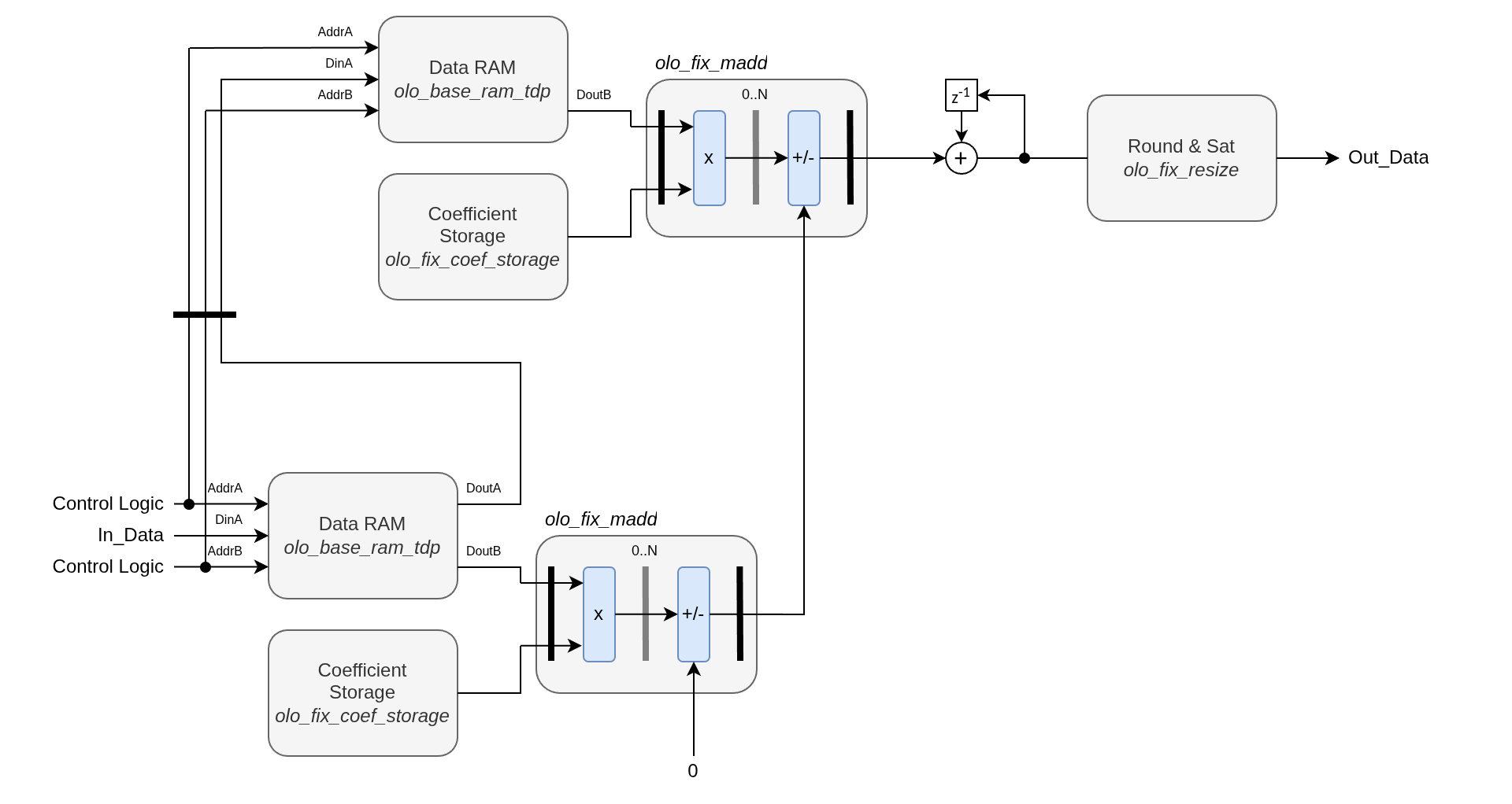
Each stage owns:
- A data delay-line RAM (olo_base_ram_tdp). The RAMs are chained so that each stage sees the input delayed by a further block of taps.
- A coefficient storage (olo_fix_coef_storage) holding only that lane's block of ceil(Taps_g / Multipliers_g) coefficients (ROM or RAM depending on CoefStorageType_g). The coefficient memory is therefore split across the stages rather than replicated, so the total coefficient memory does not grow with Multipliers_g. Coefficient writes and readbacks addressed through the Coef_... ports are routed to (and muxed back from) the stage that owns the addressed tap.
Below figure depicts a single stage of the MACC chain.
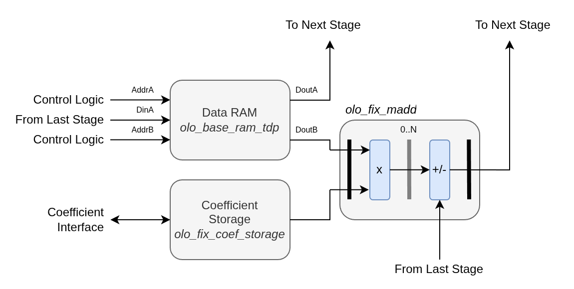
The result of the accumulation is rounded and saturated to OutFmt_g using olo_fix_resize.
The memory styles of the coefficient storage and the data RAM can be selected independently through CoefMemStyle_g and DataMemStyle_g. To minimize coefficient memory, choose a coefficient storage type that fits the use case: ROM for fixed coefficients, or RAM without readback (CoefRamReadback_g = false) when runtime updates are needed but readback is not.
Full Input Rate Support
When FullInpRateSupport_g = false (default), the chained data memory needs one idle cycle between two input samples, hence In_Valid must not be asserted on two consecutive clock cycles.
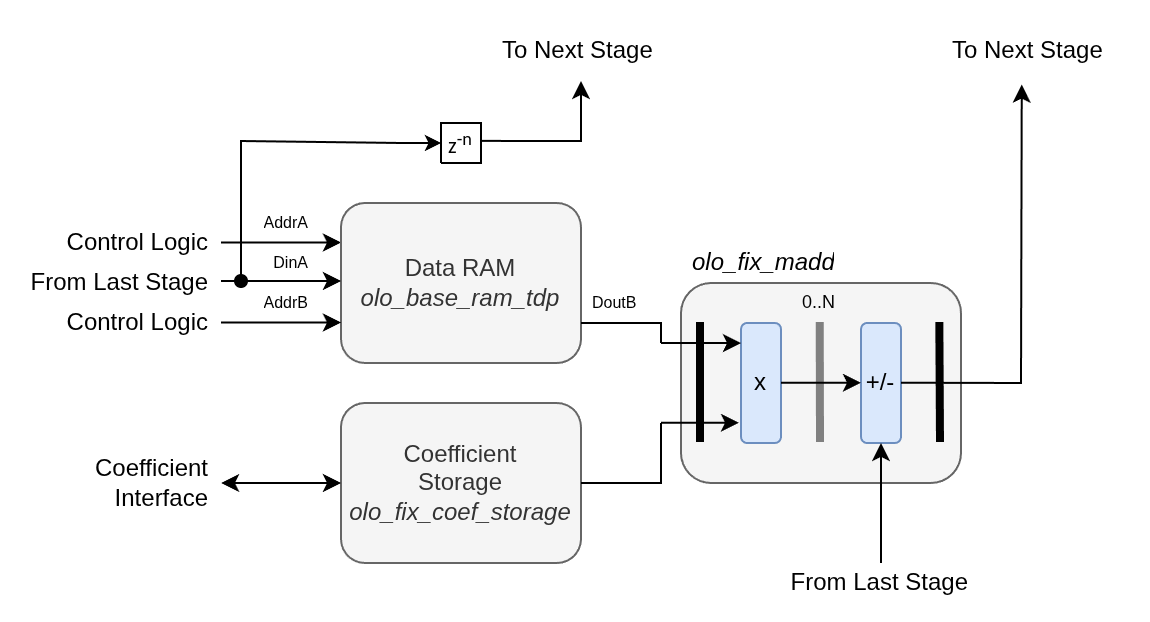
When FullInpRateSupport_g = true, an additional delay line (olo_base_delay) per stage provides the chained delay, so In_Valid may be asserted on every clock cycle. Note that this only relaxes the back-to-back input restriction; the overall processing power limit (see Input Bandwidth Limitation) still applies - and the price for the architecture is additional memory for the extra delay lines. Whenever possible it is to be preferred to avoid In_Valid being asserted on consecutive clock cycles and to use FullInpRateSupport_g = false.
The stage architecture with FullInpRateSupport_g = true is depicted below:
Startup and Flushing
The delay lines are stored in RAM and are not cleared by reset. After power-up the RAMs are zero initialized, hence the first outputs are bit-true without any special action. If the filter is reset during operation, the RAMs still contain old data. In this case a flush must be triggered (pulse Flush_Ena and wait for Flush_Done) to zero the delay lines before feeding new data. This guarantees bit-true agreement with the Python model, which initializes its delay line to zero.
Coefficient Format
The accumulator operates at full multiply precision:
- MultFmt = (max(In.S, Coef.S), In.I + Coef.I, In.F + Coef.F)
- AccuFmt = (1, Out.I + GuardBits_g, In.F + Coef.F) (GuardBits_g guard bits above output)
Choosing OutFmt.I or GuardBits_g too small risks accumulator overflow. Ensure max_sum_of_products <= 2^(OutFmt.I + GuardBits_g) - 1 LSB.
Accumulator Guard Bits
The accumulator carries GuardBits_g integer guard bits above OutFmt_g (AccuFmt.I = OutFmt.I + GuardBits_g). These bits allow the sum of products to grow beyond the output range during the accumulation without overflowing. With the default of one guard bit, intermediate results of up to twice the OutFmt_g maximum are supported. The user is responsible for choosing GuardBits_g, the coefficients and the formats such that the accumulator does not overflow; otherwise the number of guard bits or the output format must be increased.
Last Handling
On the input, In_Last is not required for operation. It is only used in simulation to detect incorrect TDM framing: an error is reported if In_Last is asserted on a sample that does not belong to the last channel (Channels_g-1). It has no functional effect on the computation.
On the output, Out_Last is generated by the entity itself and is always asserted together with Out_Valid on the last channel (Channels_g-1) of every output sample set.