olo_ft_ram_tdp
Status Information
VHDL Source: olo_ft_ram_tdp
Description
This component implements an ECC-protected true dual-port RAM using SECDED (Single Error Correction, Double Error Detection) Hamming code. It wraps olo_base_ram_tdp internally with a wider word to store parity bits alongside data.
The ECC is transparent to the user: data is automatically encoded on write and decoded/corrected on read. Error status flags indicate whether a single-bit error was corrected or a double-bit error was detected.
The true dual-port topology has two fully independent ports (A and B). Each port can read and write, each runs on its own clock (A_Clk / B_Clk), and each has its own ECC encoder and decoder so the two ports are protected independently.
This is useful in radiation-hardened designs where single-event upsets (SEUs) can flip bits in memory cells, e.g. in space or high-energy physics environments.
For background on the SECDED scheme, the codeword layout, error injection semantics and the constraints that apply across the ft area, see Open Logic Fault-Tolerance Principles.
Warning
True dual port RAM is NOT supported when compiling with Yosys for Cologne Chip FPGAs. Please use olo_base_ram_sdp instead.
Generics
| Name | Type | Default | Description |
|---|---|---|---|
| Depth_g | positive | - | Number of addresses the RAM has |
| Width_g | positive | - | Number of data bits stored per address (word-width). The internal RAM is wider to accommodate ECC parity bits. |
| RamRdLatency_g | positive | 1 | Read latency of the wrapped RAM, excluding ECC pipeline stages. Higher values can help close timing on the RAM read path. |
| RamStyle_g | string | "auto" | Controls the RAM implementation resource. Passed through to olo_base_ram_tdp. |
| RamBehavior_g | string | "RBW" | Controls the RAM behavior. "RBW": Read-before-write "WBR": Write-before-read |
| EccPipeline_g | natural | 0 | Number of pipeline register stages within each ECC decoder (range 0..2). 0 = combinational decode (default). 1 = single register at the decoder output - breaks the path from the RAM read port to the user's logic. 2 = distributed pipeline: register between syndrome compute and correction, plus a register at the output - use this when both halves of the SECDED logic need their own clock cycle to close timing. See ECC Pipeline for details. Total read latency is RamRdLatency_g + EccPipeline_g cycles. |
Interfaces
The two ports are symmetric. Port A and Port B carry the same set of signals with the A_ / B_ prefix respectively. The descriptions below are written for Port A; Port B behaves identically on its own clock.
Port A
| Name | In/Out | Length | Default | Description |
|---|---|---|---|---|
| A_Clk | in | 1 | - | Port A clock |
| A_Rst | in | 1 | '0' | Port A reset (high-active, synchronous to A_Clk). Clears the port's error-injection latch and read-valid pipeline. RAM contents are unaffected (block RAMs cannot be reset). |
| A_Addr | in | ceil(log2(Depth_g)) | - | Port A address |
| A_WrEna | in | 1 | '0' | Port A write enable |
| A_WrData | in | Width_g | 0 | Port A write data |
| A_RdEna | in | 1 | '1' | Port A read enable. A_RdValid pulses '1' exactly RamRdLatency_g+EccPipeline_g cycles after each A_RdEna = '1' cycle. The RAM always reads; A_RdEna only gates the valid flag. Leave at the default '1' for continuous reads. |
| A_RdData | out | Width_g | N/A | Port A read data (corrected if a single-bit error was detected) |
| A_RdValid | out | 1 | N/A | Port A read-data valid. Pulses '1' when A_RdData / A_RdEccSec / A_RdEccDed correspond to a read (= A_RdEna delayed by RamRdLatency_g+EccPipeline_g cycles). |
| A_RdEccSec | out | 1 | N/A | Port A single error corrected flag. '1' when a single-bit error was detected and corrected. |
| A_RdEccDed | out | 1 | N/A | Port A double error detected flag. '1' when an uncorrectable double-bit error was detected. Read data is unreliable in this case. |
| A_ErrInj_BitFlip | in | eccCodewordWidth(Width_g) | all 0 | Port A error injection. Codeword-wide flip pattern XORed into the stored codeword. Popcount 1 = SEC-correctable, popcount 2 = DED-detectable. Leave unconnected for normal operation. See Error Injection. |
| A_ErrInj_Valid | in | 1 | '0' | Port A injection strobe. Latches A_ErrInj_BitFlip into the encoder's pending-injection register; the pattern is applied to the next write. |
Port B
| Name | In/Out | Length | Default | Description |
|---|---|---|---|---|
| B_Clk | in | 1 | - | Port B clock |
| B_Rst | in | 1 | '0' | Port B reset. Same behavior as A_Rst on B_Clk. |
| B_Addr | in | ceil(log2(Depth_g)) | - | Port B address |
| B_WrEna | in | 1 | '0' | Port B write enable |
| B_WrData | in | Width_g | 0 | Port B write data |
| B_RdEna | in | 1 | '1' | Port B read enable. Same behavior as A_RdEna. |
| B_RdData | out | Width_g | N/A | Port B read data (corrected if a single-bit error was detected) |
| B_RdValid | out | 1 | N/A | Port B read-data valid. Same behavior as A_RdValid. |
| B_RdEccSec | out | 1 | N/A | Port B single error corrected flag. Same behavior as A_RdEccSec. |
| B_RdEccDed | out | 1 | N/A | Port B double error detected flag. Same behavior as A_RdEccDed. |
| B_ErrInj_BitFlip | in | eccCodewordWidth(Width_g) | all 0 | Port B error injection. Same behavior as A_ErrInj_BitFlip. |
| B_ErrInj_Valid | in | 1 | '0' | Port B injection strobe. Same behavior as A_ErrInj_Valid. |
Detailed Description
Architecture
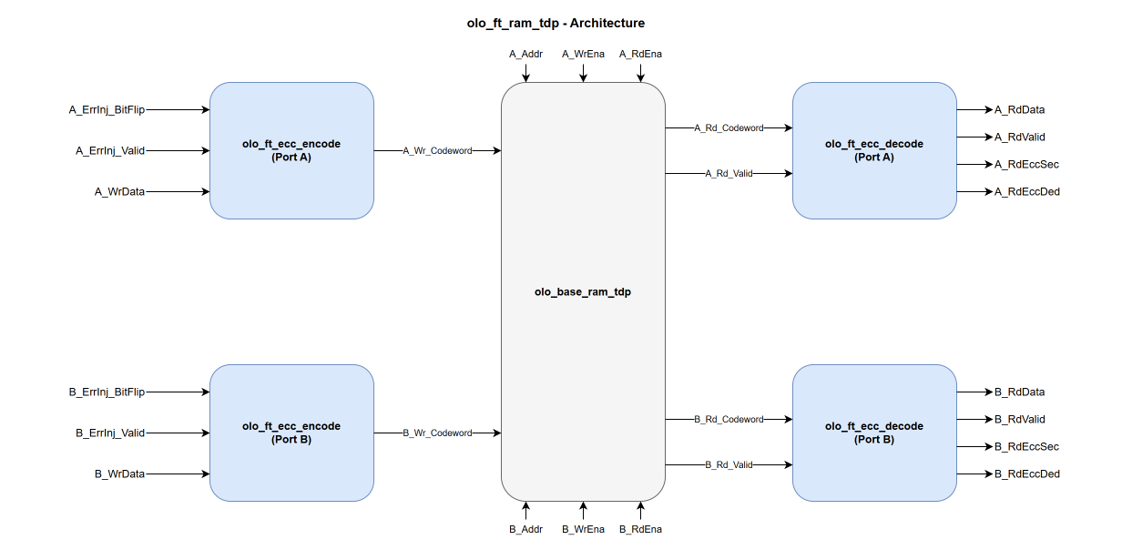
Each port has its own ECC encoder and decoder, so the two ports are protected independently and can run on
independent clocks. The ECC encoding is combinational on each write path. The internal RAM (an instance of
olo_base_ram_tdp with a codeword-wide word) provides the configurable read pipeline (RamRdLatency_g) and forwards a
per-port RdValid to the matching decoder. The ECC decoding happens in the per-port
olo_ft_ecc_decode instances and the error flags are time-aligned with the read data
regardless of EccPipeline_g.
Unlike the single- and simple-dual-port RAMs, olo_base_ram_tdp always reads on both ports; the A_RdEna / B_RdEna inputs only gate the corresponding RdValid output, they do not gate the RAM read itself.
ECC Pipeline
EccPipeline_g is forwarded one-to-one to both internal olo_ft_ecc_decode instances and
inserts register stages on the decode datapath. The range is 0..2:
EccPipeline_g |
Structure |
|---|---|
| 0 | Combinational decode after the RAM read port. A_RdData / A_RdEccSec / A_RdEccDed appear RamRdLatency_g cycles after A_Addr. |
| 1 | Combinational syndrome + correction + SEC/DED → register near the output. Breaks the path from the RAM read port to the user's logic. |
| 2 | Combinational syndrome → register → combinational correction + SEC/DED → register. Breaks both the syndrome path and the correction path - use this when both halves of the SECDED logic need their own clock cycle to close timing at high clock frequencies. |
Total read latency from address-presented to data-valid is RamRdLatency_g + EccPipeline_g clock cycles.
ECC Overhead, Error Injection and Status Flags
See the corresponding sections in Open Logic Fault-Tolerance Principles:
- ECC Overhead — internal storage width vs. data width
- Error Injection — semantics of ErrInj_BitFlip / ErrInj_Valid (per port via the A_ / B_ prefixes)
- Error Status Flags — meaning of RdEccSec / RdEccDed
Constraints
See
Open Logic Fault-Tolerance Principles - Constraints That Apply Across the Area
for the no-byte-enables and no-initialization constraints. In addition, the following olo_ft_ram_tdp-specific
constraint applies:
- True dual-port RAM is NOT supported when compiling with Yosys for Cologne Chip FPGAs (inherited from olo_base_ram_tdp).