olo_intf_spi_master
Status Information
VHDL Source: olo_intf_spi_master
Description
Overview
This entity implements a simple SPI master. All common SPI settings are configurable to ensure the master can be configured for different applications.
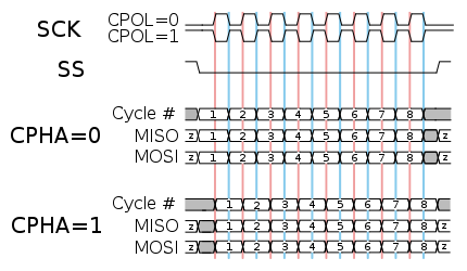
The clock and data phase is configurable according to the SPI standard terminology described in the picture below:
CPOL and CPHA meaning
For CPHA = 1, the sampling happens on the second edge (blue) and data is applied on the first edge (red). For CPHA = 0 it is the opposite way.
The number of bits to transfer can be chosen per transaction. Alternatively, the related port Cmd_TransWidth can be left unconnected - in this case, all transactions are MaxTransWidth_g bits. Similarly the slave to communicate with can be selected through Cmd_Slave for every transaction ot the signal can be left unconnected when only one slave is used - in this case all transactions implicitly are for communicating with slave 0.
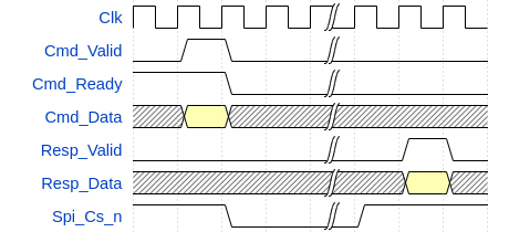
The user interface (FPGA side) is split into a command interface (Cmd...) and a response interface (_Resp..._). Below figure summarizes how they behave timing-wise.
Generics
| Name | Type | Default | Description |
|---|---|---|---|
| ClkFreq_g | real | - | Frequency of the clock Clk in Hz. For correct operation, the clock frequency must be at least 4x higher than SclkFreq_g. |
| SclkFreq_g | real | 1.0e6 | SPI clock (Sclk) frequency in Hz. |
| MaxTransWidth_g | positive | 32 | Maximum number of bits to transfer per SPI transaction. The actual number of bits to transfer for every transaction is selected through Cmd_TransWidth. If all transactions have the same width, Cmd_TransWidth can be left unconnected - in this case always MaxTransWidth_g bits are transferred. |
| CsHighTime_g | real | 20e-9 | Minimum Cs_n high time between two consecutive transactions in seconds. |
| SpiCpol_g | natural | 1 | SPI clock polarity, see figure in Overview. Range: 0 or 1 |
| SpiCpha_g | natural | 1 | SPI clock phase, see figure in Overview. Range: 0 or 1 |
| SlaveCnt_g | positive | 1 | Number of slaves (number of bits in SpiCs_n). |
| LsbFirst_g | boolean | false | True: Transactions are LSB first (data bit 0 is sent first). False: Transactions are MSB first (data bit 0 is sent last) |
| MosiIdleState_g | std_logic | '0' | State of SpiMosi when no transaction is ongoing. In most cases this does not matter. |
Interfaces
Control
| Name | In/Out | Length | Default | Description |
|---|---|---|---|---|
| Clk | in | 1 | - | Clock |
| Rst | in | 1 | - | Reset input (high-active, synchronous to Clk) |
Command Interface
| Name | In/Out | Length | Default | Description |
|---|---|---|---|---|
| Cmd_Ready | out | 1 | N/A | AXI-S handshaking signal for Cmd..._ |
| Cmd_Valid | in | 1 | - | AXI-S handshaking signal for Cmd..._ |
| Cmd_Slave | in | ceil(log2(SlaveCnt_g)) | 0 | Index of the slave to communicate with. 0 ("0000") -> Spi_Cs_n[0] is operated 3 ("0011") -> Spi_Cs_n[3] is operated The port can be left unconnected if only one slave is used. |
| Cmd_Data | in | MaxTransWidth_g | 0 | Data to send. For TransWidth < MaxTransWidth_g the data is right aligned (MSBs are unused). |
| Cmd_TransWidth | in | ceil(log2(MaxTransWidth_g+1)) | MaxTransWidth_g | Number of bits to transfer in this transaction. The port can be left unconnected if all transactions are MaxTransWidth_g bits wide. |
| Cmd_CsHold | in | 1 | '0' | If '1', Cs_n is held active after the transaction. see CS Handling |
Response Interface
| Name | In/Out | Length | Default | Description |
|---|---|---|---|---|
| Resp_Valid | out | 1 | N/A | AXI-S handshaking signal for Resp... The response interface does not support backpressure. Hence no _Ready signal is provided. |
| Resp_Data | out | MaxTransWidth_g | N/A | Data received For TransWidth < MaxTransWidth_g the data is right aligned (MSBs are unused). |
SPI Interface
| Name | In/Out | Length | Default | Description |
|---|---|---|---|---|
| Spi_Sclk | out | 1 | N/A | SPI clock (frequency selected through SclkFreq_g) |
| Spi_Mosi | out | 1 | N/A | SPI data from master to slaves |
| Spi_Miso | in | 1 | '0' | SPI data from slaves to master. Can be left unconnected if the master only does write data. |
| Spi_Cs_n | out | SlaveCnt_g | N/A | SPI chip select (one signal per slave) |
Details
Clock Frequency Calculation
The Spi_Sclk signal is implemented as data-signal (not generated through a PLL) in the FPGA.
The frequency of Spi_Sclk is calculated as follows:
Fsclk = Fclk / (2 x N)
N is an integer and chosen automatically according to ClkFreq_g and SclkFreq_g. However, the resulting clock frequency is affected by rounding. The olo_intf_spi_master does assert an error if the SCLK frequency is off by more than 10% compared to SclkFreq_g requested. To avoid this issue for SclkFreq_g values that are high, chose SclkFreq_g to be implementable according to the formula below.
CS Handling
By default (Cmd_CsHold = '0'), Cs_n is deasserted (goes high) between two transactions. In some cases this is not wanted. For example for memory devices receiving multiple write data words in a row.
By using Cmd_CsHold = '1', Cs_n is held active (low) after the transaction. If the next transaction goes to the same slave, Cs_n is kept active (low) between the two transactions.
In case Cmd_CsHold = '1' and the next transaction goes to a different slave, Cs_n is deasserted (goes high) when the next transaction is injected through the Cmd interface and hence the olo_intf_spi_master can detect the change of slave.