Cologne Chip Tutorial
Introduction
The aim of this tutorial is give users a kick-start on creating Cologne Chip projects using Open Logic.
The Cologne Chip toolchain is based on Yosys based oss-cad-suite and hence the same tutorial might apply for Yosys/oss-cad-suite in general.
The tutorial covers project setup and implementation up to the production of a running bitstream for a small design. The design is rather hardware independent but all examples and pinout constraints are given for a GateMate FPGA Starter Kit evaluation board. If you want to use it on some other hardware, just change pinout and the target device accordingly.
The steps should be very much independent of the oss-cad-suite version but all screenshots are taken with the oss-cad-suite build from Sep-2025.
Note: Instantiating VHDL entities with generics from Verilog is currently not supported by Yosys. Hence this tutorial is only available for VHDL.
Step 1: Setup Hardware
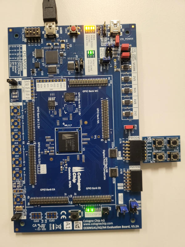
The GateMate FPGA Starter Kit does not contain the buttons required for this tutorial. Therefore a PMod BTN must be connected to the upper row of the connector PMODA as shown below.
Step 2: Build Project
Overview
In this tutorial we will build the following design:
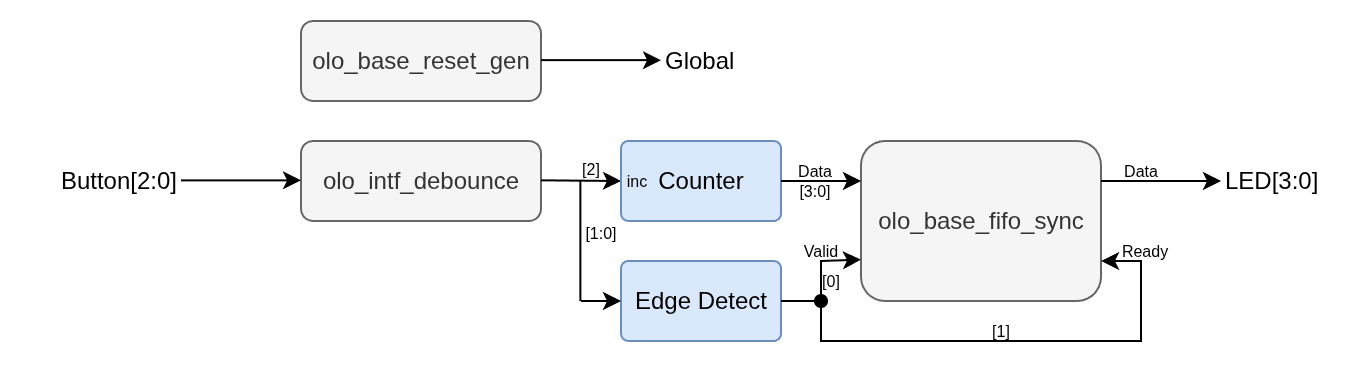
All Open Logic blocks are shown in grey. Custom logic is shown in blue.
The design does de-bounce all three buttons.
Every time the user presses Button[2], the counter is incremented. Every time the user presses Button[0], the state of the counter is written into a FIFO (4 bits wide, 4096 entries deep). Every time the user presses Button[1], one FIFO entry is read and applied to the LEDs. Note that clock and reset are not shown in the figure for simplicity reasons.
The de-bouncing is required to ensure that a button press really only produces one edge (and hence one read/write transaction to the FIFO resp. a single increment of the counter).
The design is super simple - it is not meant for demonstrating the coolest features of Open Logic but for being the simplest possible example of a design making use of Open Logic.
Build Design
Because the oss-cad-suite does not come with a GUI, in contrast to all other tutorials this tutorial does not congain a GUI walkthrough. Instead it mainly consists of the build srcipt.
Note: The build script is provided for Linux environments. For Windows, the commands must be adapted accordingly.
To build the project, first navigate to the folder <open-logic-root>/doc/tutorials/CologneChipTutorial/Files in a
shell. Then execute the build script scrtipted_build.sh:
cd <open-logic-root>/doc/tutorials/CologneChipTutorial/Files
source ./scripted_build.sh
In the build script, the only line that really is Open Logic specific is the following one:
python3 ../../../../tools/yosys/compile_olo.py
This line does compile Open Logic. All other content is as decribed on the Cologne Chip Website under the Getting Started section.

Analyze Resource Utilization
From the resource utilization (see nexpnr.log) it is obvious that the FIFO was correctly mapped to Block-RAM (one RAM_HALF is used).
Info: Device utilisation:
Info:             USR_RSTN:       0/      1     0%
Info:             CPE_COMP:       0/  20480     0%
Info:          CPE_CPLINES:      12/  20480     0%
Info:                IOSEL:       9/    162     5%
Info:                 GPIO:       9/    162     5%
Info:                CLKIN:       1/      1   100%
Info:               GLBOUT:       1/      1   100%
Info:                  PLL:       0/      4     0%
Info:             CFG_CTRL:       0/      1     0%
Info:               SERDES:       0/      1     0%
Info:               CPE_LT:     524/  40960     1%
Info:               CPE_FF:     133/  40960     0%
Info:            CPE_RAMIO:      49/  40960     0%
Info:             RAM_HALF:       1/     64     1%
The overall LUT count of the design is 524 CPE_LT. For interpreting this number it must be kept in mind, that a CP_LT is only half a LUT, hence the design uses 262 full LUTs.
Analyze Timing
The timing report shows that unsurprisingly the slow clock-speed of the 10 MHz clock is met.
Info: Max frequency for clock 'i_fifo.clk': 94.83 MHz (PASS at 10.00 MHz)
Step 3: Program Hardware
The board can be programmed by executing the command below. Note that on Linux permissions must be set correctly or alternatively the command might have to be exeuted as root.
openFPGALoader -b gatemate_evb_spi -m ./cologne_tutorial.bit
You can increment the counter (press BTN2) and write (BTN0) a few counter values into the FIFO. The values can then be displayed on the the LEDs one by one by pressing BTN1.
Step 5: Discussion of the VHDL Source Code
The source code can be found in the file \<open-logic-root>/doc/tutorials/CologneChipTutorial/Files/cologne_tutorial.vhd.
Not every line of the source code is discussed. It is simple and implements the design described earlier. Only a few details worth mentioning are discussed.
Omitting Unused Generics
The FIFO instance only sets two generics:
    i_fifo : entity olo.olo_base_fifo_sync
        generic map (
            Width_g         => 4,
            Depth_g         => 4096
        )
        ...
The olo_base_fifo_sync entity would have much more generics but due to the concept of providing default values for optional generics, it is not necessary to obfuscate source-code with many lines of actually unused generics.
entity olo_base_fifo_sync is
    generic (
        Width_g         : positive;
        Depth_g         : positive;
        AlmFullOn_g     : boolean   := false;
        AlmFullLevel_g  : natural   := 0;
        AlmEmptyOn_g    : boolean   := false;
        AlmEmptyLevel_g : natural   := 0;
        RamStyle_g      : string    := "auto";
        RamBehavior_g   : string    := "RBW";
        ReadyRstState_g : std_logic := '1'
    );
    ...
Omitting Unused Ports
The same concept applies to unused ports. In this case we do neither require full handshaking nor status signals like Full/Empty/Level - hence all these signals can be omitted:
    i_fifo : entity olo.olo_base_fifo_sync
        ...
        port map (
              Clk           => Clk,
              Rst           => Rst,
              In_Data       => Data,
              In_Valid      => RisingEdges(0),
              Out_Data      => Led,
              Out_Ready     => RisingEdges(1)
        );
Again compared to the full list of signals the olo_base_fifo_sync provides many lines of obfuscating code can be omitted because all optional input ports come with default values.
entity olo_base_fifo_sync is
    ...
    port (
        -- Control Ports
          Clk           : in  std_logic;
          Rst           : in  std_logic;
          -- Input Data
          In_Data       : in  std_logic_vector(Width_g - 1 downto 0);
          In_Valid      : in  std_logic                                             := '1';
          In_Ready      : out std_logic;
          In_Level      : out std_logic_vector(log2ceil(Depth_g + 1) - 1 downto 0);
          -- Output Data
          Out_Data      : out std_logic_vector(Width_g - 1 downto 0);
          Out_Valid     : out std_logic;
          Out_Ready     : in  std_logic                                             := '1';
          Out_Level     : out std_logic_vector(log2ceil(Depth_g + 1) - 1 downto 0);
          -- Status
          Full          : out std_logic;
          AlmFull       : out std_logic;
          Empty         : out std_logic;
          AlmEmpty      : out std_logic

    );