olo_base_ram_sp
Status Information
VHDL Source: olo_base_ram_sp
Description
This component implements a single-port RAM.
The RAM is implemented in pure VHDL but in a way that allows tools to implement it in block-RAMs.
Generics
| Name | Type | Default | Description |
|---|---|---|---|
| Depth_g | positive | - | Number of addresses the RAM has |
| Width_g | positive | - | Number of bits stored per address (word-width) |
| UseByteEnable_g | boolean | false | By default, all bits of a memory cell are written. Enabling byte-enables allows to control which bytes are written individually. The setting is only allows for if Width_g is a multiple of eight (otherwise the word byte-enable does not make sense). Note that setting this setting to true can lead to increased resource usage. See Detailed Description |
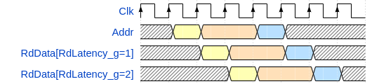
| RdLatency_g | positive | 1 | Read latency. 1 is the behavior of a normal synchronous RAM Higher values can be desirable for timing-optimization in high-speed logic. |
| RamStyle_g | string | "auto" | Through this generic, the exact resource to use for implementation can be controlled. This generic is applied to the attributes ram_style and ramstyle which vendors offer to control RAM implementation. Commonly used values are given below. AMD: "auto", block", "distributed", "ultra" - see ug901 for details Altera: "M4K", "M9K", "M20K", "M144K", "MLAB" - see quartus-help for details Efinix: "block_ram", "registers" - see efinity-synthesis for details Synplify(Lattice/Microchip): "block_ram", "registers", "distributed" - see microchip-attributes-guide for details Gowin: "block_ram", "distributed_ram", "registers", "rw_check", "no_rw_check" - see GowinSynthesis User Guide for details. |
| RamBehavior_g | string | "RBW" | Controls the RAM behavior. Must match the behavior of RAM resources of the target technology for efficient implementation. "RBW": Read-before-write - more common common, hence the default "WBR": Write-before-read If you are unsure what behavior your target device offers, try both settings and check which one is correctly mapped to RAM resources using the synthesis report. |
| InitString_g | string | "" | Initialization data for the memory formatted as comma separated list of hex calues (e.g. "0x1234, 0x0ABC"). Each value MUST have the 0x prefix. The first value goes to address 0, the second one to address 1 and so on. |
| InitFormat_g | string | "NONE" | "NONE": RAM is not initialized "HEX": RAM is initialized with InitString_g interpreted as list of hex values. Note: Not all technologies support RAM initialization. Check the documentation of your technology/tools for details. |
Interfaces
| Name | In/Out | Length | Default | Description |
|---|---|---|---|---|
| Clk | in | 1 | - | Clock |
| Rst | in | 1 | '0' | Synchronous reset Optional, only resets internal state of RdValid Does NOT reset the content of memory cells! |
| Addr | in | ceil(log2(Depth_g)) | - | Address |
| Be | in | Width_g/8 | All '1' | Byte-enables Ignored if UseByteEnable_g = false |
| WrEna | in | 1 | '1' | Write enable. The memory cell at Addr is written only if WrEna='1'. |
| WrData | in | Width_g | - | Write data |
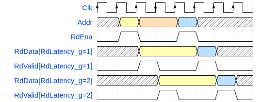
| RdEna | in | 1 | '1' | Read enable. When asserted, RdData is updated and RdValid is asserted after RdLatency_g cycles. |
| RdData | out | Width_g | N/A | Read data |
| RdValid | out | 1 | N/A | Read valid. Asserted RdLatency_g cycles after RdEna was asserted. |
Detailed Description
Read Latency
Below figure explains the RdLatency_g generic in detail:
Byte Enables
Due to tool limitations regarding inference, the usage of byte enables (UseByteEnable_g=true) can lead to increased RAM usage. Therefore, do not use byte enable signals unless this is strictly required.
Open Logic internally does not use byte enables, hence only users using the olo_base_ram_sp component directly with byte-enables enabled are affected.
For applications where vendor/tool independence is important, this is to be regarded as a required trade-off. For applications that target only one specific technology, it is suggested to use vendor macros if RAM with byte enables if required.
RdEna and RdValid
The RAM is read and RdData is updated only when RdEna signal is asserted.
Besides controlling RAM read operations, the RdEna signal controls the RdValid signal. This means that if RdEna is asserted, RdValid is asserted after RdLatency_g cycles, indicating that the data on RdData is valid and can be used. This is very useful in pipelined design, especially with configurable RdLatency_g values because it allows to design logic around independently of the RAM read latency.